Taiwan Semiconductor Manufacturing Company's (TSMC) second Japan-based manufacturing facility faces setbacks, with mass production now scheduled for 2029.
The construction of TSMC's Fab 23 phase 2 (also known as JASM phase 2) in Kumamoto, Japan, has encountered a delay of up to 18 months due to local traffic congestion and inadequate infrastructure around the site. This delay will shift the start of mass production from the late 2027 originally planned to 2029, with the first commercial products not expected to be manufactured until around 2028–2029 at the earliest.
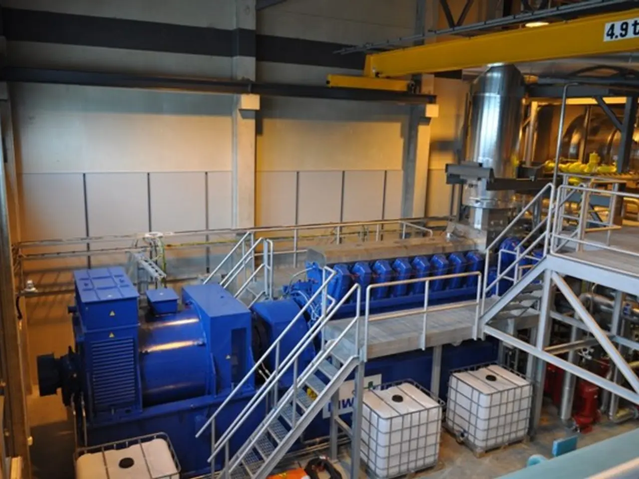
The traffic congestion problem has hindered the delivery of thousands of tons of construction materials and specialized equipment such as Low-NA EUV tools, which are critical for the fab's advanced N7/N6 capabilities. The delay is linked specifically to local infrastructure readiness rather than strategic shifts in TSMC’s investment plans. TSMC CEO C.C. Wei has emphasized that construction timing depends on "local infrastructure conditions," customer demand, and market factors.
This delay complements TSMC’s broader international strategy involving facilities in Japan, the US, Taiwan, and Germany, driven by semiconductor demand, especially for AI-related chips. However, it reflects challenges in global supply chain logistics, particularly in congested areas.
The postponement could potentially affect supply timelines for advanced chips targeted to the automotive and electronics sectors in Japan, where TSMC, Sony, and Denso collaborate through the JASM joint venture.
Despite the delay, a Japanese government official has expressed scepticism about traffic congestion being the cause of the delay but expects the fab’s production schedule and capacity targets to largely stay on track. TSMC began mass production at Fab 23 phase 1 in late December 2024.
It is worth noting that fabs are 24/7/365 facilities that consume high-purity chemicals. High-purity chemicals must be delivered on time to avoid costly production disruptions. Furthermore, these chemicals must be delivered safely to avoid opposition from locals. Typically, it takes 18 to 24 months from pouring the foundation to the first test wafers running around the fab.
Transporting these massive pieces of equipment in congested areas can be challenging and drive up costs. In addition, the transportation of delicate equipment in congested areas increases the risk of accidents. Special logistics for Low-NA EUV tools can also be challenging in such areas.
In conclusion, the primary reason for the delay is transportation and infrastructure bottlenecks near the construction site, which impacts the supply chain for heavy construction and specialized semiconductor manufacturing equipment logistics. This causes an about 1.5-year setback in construction and mass production start, moving commercial chip output to 2028–2029 instead of late 2027.
The delay in TSMC's Fab 23 phase 2 construction, caused by transportation and infrastructure issues, has resulted in a shift of the start of mass production from late 2027 to 2029, affecting the finance sector with potential delays in the supply of advanced chips. This delay also demonstrates the challenges in technology-intensive manufacturing industries, where the delivery of specialized equipment such as Low-NA EUV tools is critical.


%20second%20Japan-based%20manufacturing%20facility%20faces%20setbacks%2C%20with%20mass%20production%20now%20scheduled%20for%202029.)